Micro and Nano Processing | Preparation of Micro and Nano Optical Components
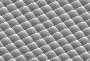
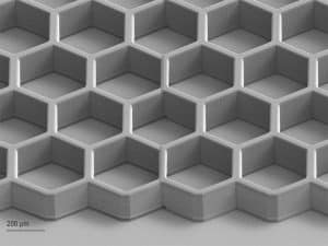
Micro and nano optical components are free-form optical surfaces and microstructured optical components with sub-micron precision and nanometer surface roughness. Due to their small size, light weight, flexible design, easy arraying and batch reproducibility, they can perform new functions that cannot be achieved by traditional optical elements and can form many new optical systems. At present, micro-optical element arrays have been successfully applied in various fields of modern optics, and have very important application prospects in military and aerospace, so the preparation of micro-nano-optical elements has also become an important hot research direction in the field of surface micromachining.
The preparation methods for micro and nano optical elements are divided into two main categories:
One is the ultra-precision machining technology, which mainly uses the tool to change the shape of the material or destroy the surface layer of the material to achieve the required shape in the form of cutting. The advantages of these methods are simple processing and the ability to process complex three-dimensional micro and nano structures, but the disadvantages are high processing costs, limited processing range, only suitable for processing Al, Cu and PMMA polymethyl methacrylate and a few other materials, and low processing efficiency, it is difficult to achieve array-type devices and large-scale cheap replication, but also not easy to produce non-rotationally symmetric optical components;
The other category, which is also the mainstream technology for the preparation of micro and nano optical components, is an optical processing method that combines a variety of modern micro and fine processing technologies. The most representative ones are binary optical technology and direct writing technology for micro and nano optical components. The advantages of optical processing methods are that they can process any irregular surface lens (especially binary optics) and can be reproduced on a large scale, but the main disadvantage is that the processing process steps are complicated and the processing cost is high, especially for some important optical materials, such as quartz, GaAs processing with continuous smooth complex three-dimensional structure still exists a large difficulty.
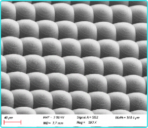
Binary optics technology combines modern processing technologies such as lithography, mask, etching and coating technology, and is the mainstream technology for preparing diffractive micro and nano optical components. If the binary structure can be obtained after one lithography, development and etching (after dry etching mainly), similarly, after n times of lithography, n times of 2 steps can be obtained, and by making multiple steps, high efficiency micro and nano optical components can be obtained. Figure 1.8 shows an electron microscope photograph of a phase-focal plane microlens array prepared by the binary optics technique.
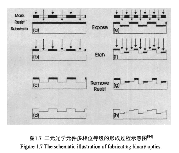
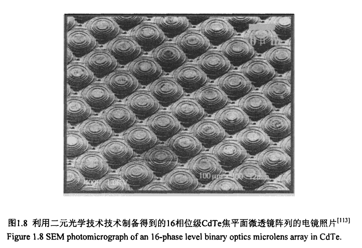
The advantages of the binary optics technique are that it cleverly overcomes the difficulties encountered in processing a continuous phase shape, opens up a novel and very important direction for the preparation of highly efficient diffractive micro and nano optical components, and can be processed on a wide range of materials. The main disadvantage of this method is that it requires several steps of sizing, baking, developing, etching, debinding, cleaning, etc., and therefore it is necessary to overcome the alignment problem caused by making the pattern on the substrate with the existing pattern in the process of multiple sizing, and it is an expensive and difficult process to add a step to obtain an optical element with high diffraction efficiency due to the expensive process equipment and complicated processing steps.
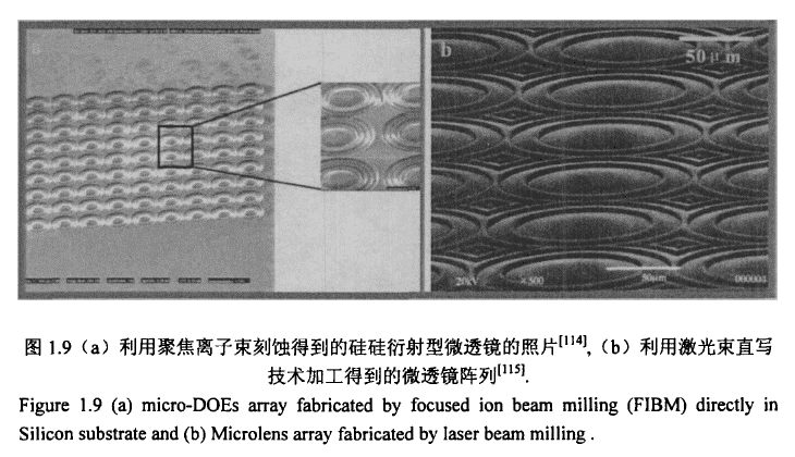
The direct writing technology of micro and nano optical components integrates various direct writing technologies, including electron beam direct writing technology, laser beam direct writing technology, focused sub beam processing and halftone mask imaging, and combines replication technology and electroforming technology to produce a variety of diffractive and refractive micro and nano optical components. The main preparation process is firstly, the computer scanning system controls various direct writing techniques on the surface of different materials, such as glass, quartz, silicon, GaAs, Cu, Al and photoresist surface processing with transverse characteristic resolution better than 5um, high resolution better than the continuous surface relief of the imperial nano structure, with these characteristics of relief microstructure materials can be directly used as micro and nano optical components (such as, quartz, silicon, GaAs, Al and photoresist). The materials with these characteristic relief microstructures can be directly used as micro and nano optical components (e.g., quartz, silicon, GaAs, Cu, Al, etc.) or further transferred to other materials such as photoresists through electroforming and replication technologies for mass production.The main advantage of the direct writing technique for micro and nano optical components is that it enables the fabrication of continuous surface relief microstructures, avoids the complex processing steps of the binary optical method, and solves the alignment problems caused by multiple exposures in the binary optical method. However, the main disadvantage of the method is that it introduces the point-by-point processing method, which is relatively slow, and the equipment required for direct processing is very expensive. Figure 1.9a shows a photograph of a silicon diffractive microlens obtained by focused ion beam processing, and Figure 1.9b shows a microlens array obtained by laser beam direct writing technique.
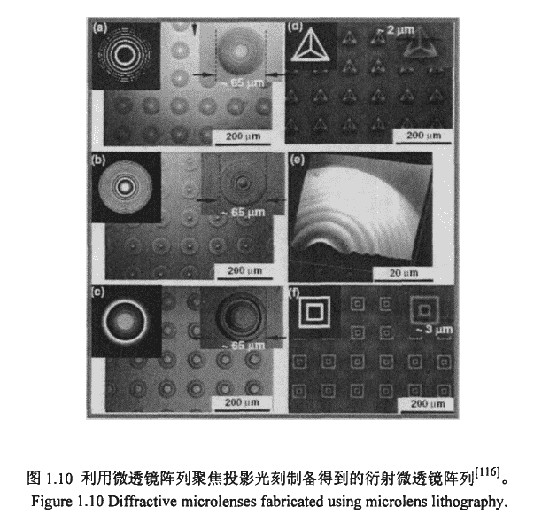
In addition, Whitesides et al. proposed a method based on microlens lithography to prepare micro-optical arrays on PDMS polydimethylsiloxane material. The microlens array with microhemispherical structure is firstly prepared on the surface of photoresist by photolithography and thermal fusion, and then the light from the original mask is further focused on the surface of another photoresist by using this microlens array, so that the surface area of the photoresist is exposed and developed to obtain a microstructure array with the same shape as the original mask but with a much smaller size, which is finally replicated by PDMS. PDMS micro-optical components with special optical applications can be obtained. The main disadvantage of this method is that it is limited to PDMS, a highly malleable polymer material, and most important optical materials, such as GaAs and quartz, cannot be processed. Figure 1.10 shows the diffractive microlens array prepared by focusing projection lithography using microlens array.
This article is extracted from "Novel electrochemical processing methods for the preparation of three-dimensional micro and nano structures on semiconductor and metal surfaces and their applications》, Xiamen University, Tension. For more information, please see the original article.
We offer fastMicro and Nano Optical Components / Micro and Nanostructure Processing Design Services, Feel free to leave a message to inquire.
Related Products
Related Reading
Micro and Nano Processing | E-paper micro-cups and micro-chamber structure preparation
Microfabrication | E-paper microcups microchamber type structure preparation For when
Micro-Nano Processing | Introduction to Wet Cleaning
Micro and Nano Processing | Introduction to wet cleaning treatment IC process requires some
Micro and Nano Processing | Photolithography - Optical Lithography
Micro and Nano Processing | Photolithography - Optical Lithography in Nano and Micro Processing Technology

