Micro-nano structure/MEMS foundry platform technology capability
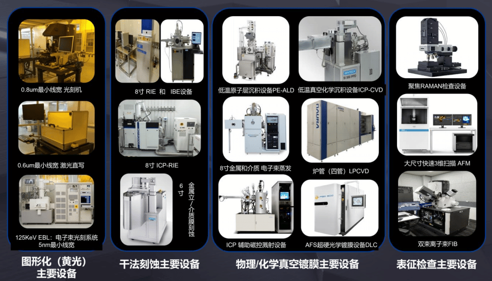
The laboratory platform has a total of more than 200 sets of equipment, etc., of which the main equipment (more than 40 sets) includes.
-Graphical devices
Electron beam exposure, laser direct writing, desktop contact lithography, desktop lithography, etc.
-Film deposition equipment
ICP-PECVD, LPCVD, magnetron sputtering, electron beam evaporation coating, PE-ALD, DLC thin film deposition, etc., electroplating (Au, Ag, Cu, Ni, Sn, etc.)
-Etching equipment
ICP-RIE, RIE, IBE, DRIE deep silicon etching, XeF2 table silicon etching machine, HF vapor phase etching and other dry etching equipment and wet etching equipment to meet the body silicon, dielectric film, metal oxide, metal, etc. and the matching CO2 supercritical release equipment
-Characterization and test equipment
AFM, step meter, Raman spectroscopy, SEM, FIB, confocal microscope, white light interferometer, infrared thermal imager, FEMTO-TOOL micro and nano mechanics tester, ultra-high speed camera, 3D Doppler laser vibrometer, DC/RF probe stage (60GHZ), network analyzer (60GHz), semiconductor analyzer, impedance analyzer and high-precision electrical original meter, etc.
-Device back-end packaging equipment
Wafer thinning, CMP polishing, wafer bonding, placement machine, scribing machine, wire bonding machine, solid state machine, laser welding machine and other processing equipment developed by the team, packaging equipment.

-Process integration and platform capabilities
-Conductive DLC film layer (super slip vice, conductive super hard film layer, etc.)
-AIN/PZT thin film process (piezoelectric drive material)
-Large size highly oriented carbon material growth and device processing process
-Bonding: anodic bonding, glass solder bonding, eutectic bonding (AIGe), diffusion bonding process
-Atmosphere or vacuum encapsulation, Reseal
-Grind thinning and atomic level polishing process
-Si-based all-wet micro and nano processing process - Flexible substrate micro and nano device processing
-Manufacturing and Packaging Capabilities
-Silicon through-hole (TSV) Glass through-hole (TGV)
-Pressure/Gas/Infrared/Humidity sensors
-Microfluidic chip processing and related testing
A super-slip RF / inertial device processing capabilities
-Die's full packaging capabilities
| Application Category | Equipment name | Equipment Model | Process Parameters |
| Plating | Low Pressure Chemical Vapor Deposition (LPCVD) | HORIS L6471-1 | Can deposit SIN, TEOS, poly and other thin Film 1-50 pieces/oven |
| Thermal oxidation | Thermal oxidation of furnace tubes | ||
| Annealing | Rapid annealing furnace RTP | Annealsys AS-One 150 | Maximum temperature up to 1500°C, temperature rise rate Max. 200℃/s |
| FIB processing | Focused Ion Beam FIB | Thermo Fisher Scios 2 HiVac | |
| TEM sample preparation | |||
| SEM morphological observation | Field Emission Environmental Scanning Electron Microscopy ESEM | Thermo Fisher Quattro S | |
| SEM energy spectrum analysis | |||
| Electron Beam Evaporation Coating - Metal | Electron beam evaporation | FU-20PEB-950 | Evaporation of metal film, can do lift-off process coating, 8-inch substrate downward compatible |
| Electron Beam Evaporation Coating - Dielectric | Electron beam evaporation | FU-12PEB | Vaporized media film can be plated 10 pieces of four-inch substrate in one furnace |
| Magnetron Sputtering Coating - Metal | Magnetron sputtering system | fse-bsls-rd-6inch | Sputtered metal film, 6" substrate |
| Atomic layer deposition | Plasma Enhanced Atomic Layer Deposition System | ICPALD-S200 | Currently dominated by Al2O3 |
| DLC coating | Diamond-like thin film chemical deposition system | CNT-DLC-CL200 | |
| Dry Etching | Dry etching machine | North Huachuang | Silicon Bosch and ultra-low temperature etching, SiO2 with quartz deep etching, below 8 in |
| IBE etching | Ion Beam Etching System (IBE) | AE4 | Three-dimensional structure material etching, etching steepness better than 85 degrees, etching accuracy 10nm |
| Plasma debinding | Microwave plasma debinding machine | Alpha Plasma | |
| UV lithography | UV Lithography | SUSS MA6BA6GEN4 | Alignment accuracy: ±0.5um, resolution 600nm |
| Electroplating | Plating Machine | WPS-200MT | Cu plating, Au plating, Ni/Ni alloy plating |
| Critical drying | Supercritical point dryer | Automegasamdri-915B | |
| Zoning | Cutting machine scribing machine | Disco D323 | |
| Wafer Bonding | Wafer Bonding Machine | SUSS MicroTec SB6Gen2 | Anode bonding |
| AFM Testing | High-resolution atomic force microscope | Oxford Cypher ES | |
| Atomic force microscopy | Park Systems NX20 | ||
| Electron beam lithography | Electron beam lithography | Elionix ELS-F125G8 | Not including the cost of glue leveling, etc., material costs are calculated separately according to the type of glue used |
We offer fastMEMS device / micro and nanostructure processing design services, Feel free to leave a message to inquire.
Related Products
Related Reading
Micro and Nano Processing | Introduction to Diffractive Optics
Micro and Nano Processing | Introduction to Diffractive Optics Diffractive Optics (Di)
Micro and Nano Processing | Microfluidic Chips
Micro and Nano Processing | Microfluidic Chips Microfluidic chips have become the most popular in single fine
Micro and Nano Processing | MEMS Micro Energy System Preparation
Micro-Nano Processing | MEMS Micro-Energy Device System Preparation With the micro-computer


