UV-LIGA Electroforming | Manufacturing Metal Array Stencil
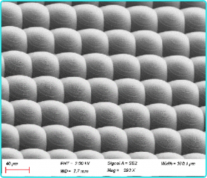
At present, the main process technologies for preparing fine metal stencil are: photolithography-etching, laser processing and photolithography-electroforming. The photolithography-etching method with chemical or electrochemical dissolution as the main process has high processing efficiency and smooth structure surface, but it is difficult to produce high aspect ratio and high resolution microstructure due to the isotropic etching behavior of the metal. Laser processing is a non-contact processing method with fast processing speed and easy automatic control, but the roughness of the processed wall surface and the existence of remelting layer limit its application in the processing of fine graphic structures with low precision. The mesh plate prepared by photolithography-electroforming process tends to have high accuracy and unrestricted hole shape with smooth walls and large opening rate. This technology is currently the main processing method for manufacturing high-performance fine metal mesh sheet in the industry is quite concerned.

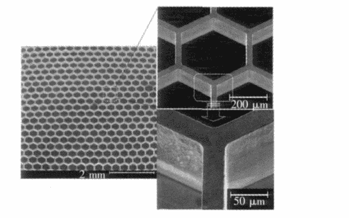
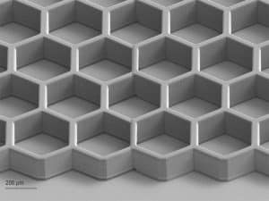
Fine metal mesh panels with regular dense array of tiny group holes are widely used in chemical fiber, precision instruments, aerospace and other fields. Such as textile industry spinnerets and printing mesh, fine filter mesh, particle sieving mesh, vacuum fluorescent display grid, surface mount meshThe mesh panels are used in the production of inkjet printer nozzles, etc. Porosity refers to the percentage of mesh area per unit area and is an important technical indicator of mesh panels. High porosity is of great relevance for certain applications of metal mesh panels. For example, the higher the open aperture rate, the higher the filtration (sieving) efficiency of the metal filter (screen) mesh overflow. However, under the established mesh shape characteristics and process conditions, the increase in perforation is often limited by the thickness of the mesh to be made. The larger the open aperture rate, the smaller the width of the tendons, the greater the height to width ratio of the structural characteristics of the tendons (the ratio of plate thickness to the width of the tendons). On the other hand, under certain conditions, the greater the thickness of the mesh plate, the greater the performance and life of the mesh plate is guaranteed. However, in the reality of production is limited to the existing manufacturing technology process capabilities, have to compromise between the perforation rate and the thickness of the balance. To explore the preparation process of high performance fine metal mesh with large thickness and high porosity is still one of the important research topics in the related industry and academia, and the fundamental problem is to solve the manufacturing problem of high aspect ratio metal microstructure characteristics.
UV-LIGA technology based on SU-8 adhesive is a low process cost high aspect ratio microstructure fabrication technology that has been rapidly developed in recent years, mainly including lithography, micro electroforming and plastic casting, etc. The 3 process steps are a new expansion of the above combined lithography-electroforming process technology. It has strong process capability in manufacturing high aspect ratio fine metal structures and devices, based on which micro coils, micro probes, micro flow channels, micro switches, micro reactors and other metal microfabrication devices have been fabricated.
UV-LIGA technology uses deep ultraviolet light from conventional exposure machines for IC manufacturing instead of synchrotron X-rays to lithograph thick glues to obtain glued microstructures, which are then used as electroforming molds for metallization and de-gluing to obtain the desired metal microstructures. UV-LIGA extends the several micron lithography process in IC production to the tens or even hundreds of micron thick lithography, and still retains the high precision and high resolution in IC process. Compared with LIGA technology, it can obtain microstructures with high aspect ratios while greatly reducing the equipment requirements, based on which micro coils, micro probes, micro flow channels, micro switches, micro reactors and other metal micro devices have been fabricated. Moreover, the compatibility with IC production lines is also much better than that of LIGA technology, thus greatly reducing the production cost and gaining more and more attention.
| LIGA Technology | UV-LIGA technology | |
| Light source | Synchrotron X-ray | Conventional UV light (wavelength of 350~450nm) |
| Mask template | X-ray mask template with Au as absorber | Standard Cr mask template |
| Photoresist | Commonly used polymethyl methacrylate PMMA | Positive and negative photoresists, polyimide, SU-8 adhesive |
| Aspect Ratio | Generally >100, up to 500 | General>10,up to 50 |
| Thickness of rubber mold | Tens of microns to several centimeters | A few microns ~ several millimeters |
| Production costs | Very high | is lower, about 1% of the left one |
| Sidewall verticality | Can be greater than 89.9° | Up to 88° |
| Minimum size | Submicron | 1~several microns |
| Processing temperature | Room temperature to about 5° | Room temperature to about 5° |
| Processing materials | Various materials such as metal, ceramic and plastic | A variety of metals, ceramics and plastics |
We offer fastMEMS device / micro and nanostructure processing design services, Feel free to leave a message to inquire.
Related Products
Related Reading
Micro and Nano Processing | Microfluidic Chips
Micro and Nano Processing | Microfluidic Chips Microfluidic chips have become the most popular in single fine
Micro and Nano Processing | Thin Film Preparation - Epitaxy
Thin Film Preparation - Epitaxy Most materials are amorphous, crystalline or polycrystalline in shape.
Micro and Nano Processing | For Cellular Arraying
Micro and Nano Processing | for Cellular Arraying Cellular Microarraying (or


