[System Introduction]
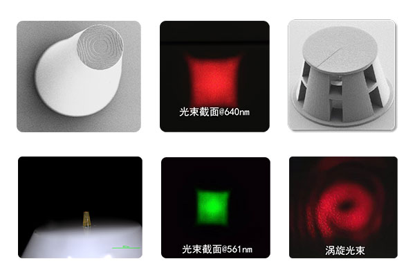
The biggest difference between the MPP-4E and a conventional two-photon laser lithography system is the use of two processing beams. One way is a femtosecond laser with a wavelength of 532nm, called the excitation light; the other way is a continuous laser with a wavelength of 532nm, called the suppression light. In the processing, the use of special PPI photoresist, this photoresist on the excitation light and inhibitory light has a different photosensitive effect: excitation light can make photoresist irradiation position occurs two-photon polymerization to form a structure, inhibitory light can destroy the photoresist molecules crosslinked to achieve the effect of de-polymerization. When the inhibitory light and excitation photosynthesis beam, through the focusing of the formation of 3D dark spot to reduce the equivalent spot size of the excitation light, so as to exceed the optical diffraction limit, to achieve high-precision dual-beam direct writing processing.
基于边缘光抑制(PPI)的激光直写技术是一种高精度三维直写光刻技术。本系统利用可见光曝光实现亚50nm尺寸结构加工,突破衍射极限,并实现单波长激发与抑制,避免色差影响,为大面积超分辨刻写奠定了研究基础。
[System parameters]
| Model | MPP-4E |
| 特征线宽 | ≤50nm (XY plane) and ≤300nm (Z axis) |
| 周期(XY平面) | ≤400nm |
| Scanning speed (maximum) | 10m/s divided by objective magnification (example: 100mm/s scanning speed at 100X objective) |
| 粗糙度 | ≤30nm |
| Print Height | ≤10mm |
| Splicing accuracy | ≤100nm (XY plane) |
| Supported engraving area (circle) | 4 inches in diameter (customizable) |
[Direction of application]
- Optics: Fresnel lenses, flash gratings, microlens arrays, etc.
- material science
- mechanical metamaterials
- Photonic chip coupling device
- Micromechanical-propeller arrays
- Photonic Lead Structure
- Biomedical: Biological Cell Scaffold Arrays
- fiber end face
- Complex space topology
- High-end Anti-counterfeiting
- Nanoimprinted stencils, masks
[Self-developed photoresist type and performance]
| Photoresists | CD (nm) | Refractive index | Wavelength(nm)/mode | Application | Sensitivity mJ/cm2 |
| Ref.IP-dip | >150 | 1.52 | 780 / DIP-IN | TPP 3D | 10 |
| TPP-1.52N | 150 | 1.52 | 517-800 / DIP-IN | TPP 3D | 8 |
| TPP-1.52S | 100 | 1.52 | 517-800 / DIP-IN | TPP 3D | 6 |
| TPP-1.56C | 100 | 1.56 | 517-800 / DIP-IN | TPP 3D Optical | 25 |
| TPP-1.56V | 180 | 1.56 | 517-800 / DIP-IN | TPP 3D Optical | 20 |
| PPI-1.48N | 50 | 1.48 | 517-800 / OIL | PPI 3D | 35 |
| PPI-1.52N | 50 | 1.52 | 517-800 / DIP-IN | PPI 3D | 7 |
| PPI-1.52S | 30 | 1.52 | 517-800 / DIP-IN | PPI 3D | 5 |
| Ref. SU-8 2000 | 500 | Solid | <350 nm | 2D | 240-600 |
| Ref. AZ 1500 | 500 | Solid | 310-450 nm | 2D | 80-130 |
| TPP-sEo | 100 | Solid | 517-800 / OIL AIR | 2D | 18 |
| TPP-sCAB | 80 | Solid | 517-800 / OIL AIR | 2D | 6 |
| TPP-sZn | 50 | Solid | 517-800 / OIL AIR | 2D | 53 |
Fresnel lens
Shining Lenticular
.jpg)
[Fiber optic end face machining]