Lithography-Photolithography
What is photolithography
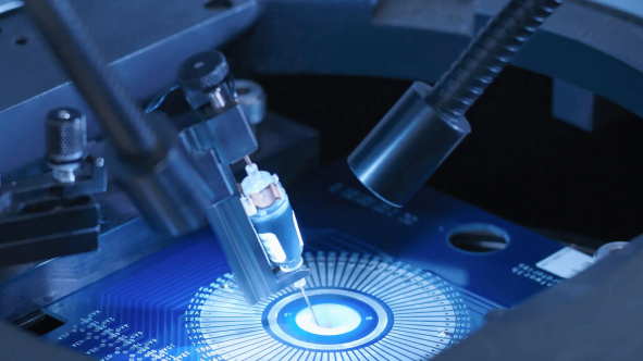
Photolithography is a precision process for patterning parts on thin films or substrates (also known as "wafers"). Photolithography uses light to transfer geometric patterns from a photomask (also known as a "photomask") to a light-sensitive (i.e., photosensitive) chemical photoresist on a substrate.
Our Capabilities
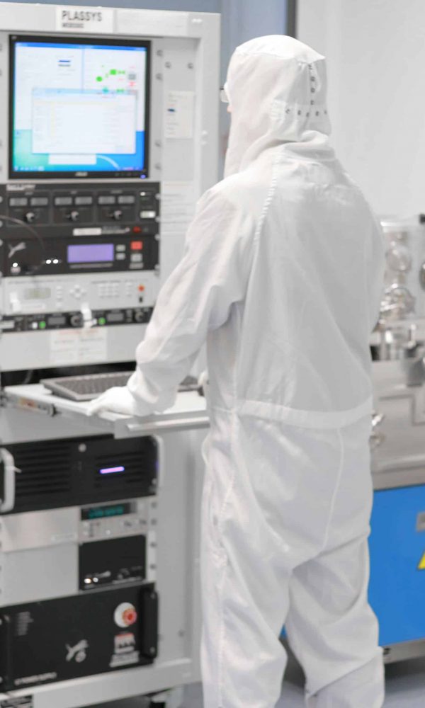
Contact and proximity Lithograph
Minimum graphic size: 1μm, scribing accuracy: ±0.5μm
Laser direct writing
(Laser direct writing)
Femtosecond laser, two-photon polymerization 3D printing.Minimum graphic size 0.3um, scribing accuracy: ±0.5um;
Lithography process
Stepper Lithography
(Stepper Lithography)
Minimum graphic size: 200 nm, registration accuracy ≤ 0.15μm (X,Y), exposure range <22*22mm, support 8inch
Lithography process
Electron Beam Lithography (EBL)
Min. graphic size: 10nm, scribing accuracy: 40nm, exposure range < 100mm diameter
Lithography process
Scanning lithography
(Scanning Lithography)
Projection ratio 1:5, the minimum graphic size: 0.35μm, set of engraving accuracy ≤ 0.15μm (X,Y), exposure range <22 * 22mm
Lithography process
Ion Beam Lithography
(Ion beam lithography)
Minimum graphic size: 1μm, scribing accuracy: ±0.5μm
Lithography materials
Lithography materials
Common substrate materials
Silicon wafers, glass, sapphire, flexible materials, GaAs, etc.
Lithography materials
Substrate size
2, 4, 6, 8 inches and irregular small pieces
Production Process
1. Preliminary offer
Send your drawings and requirements to our development manager for an initial quote
2. Program determination
We will optimize and determine the plan and quotation based on the drawings and requirements
3.Production and quality control
We will select the best equipment for your product and take full responsibility for your product to meet our standards.
4. Delivery on time
Delivered to you on time
Quality Inspection
Detection means
Optical microscopy (Microscopy)
Detection means
Profilometer (Profilometer)
Detection means
Sheet Resistance Measurement
Detection means
Hall measurement )
Cases we have done
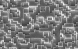
Micro and nano structures
Diffractive Optical Elements (DOE)
Micro and nano structures
Superlenses (METALENSES)
Micro and nano structures
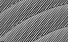
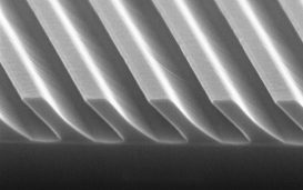
Diffraction grating (line point, shine, tilt)
Micro-Nano Architecture
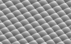
Microlens arrays
Applications

Micro and Nano Applications
Microlens arrays
Micro and Nano Applications
Line grid polarizer
Micro and Nano Applications
Sensors

Micro and Nano Applications
Flexible Electronics

Micro and Nano Applications
Anti-reflective film
Micro and Nano Applications
OLED Panel

Micro and Nano Applications
Microfluidic channels/chips

Micro and Nano Applications
AR Optical Waveguide
Our Advantages
Full process coverage
Cooperate with many domestic experiments and have different processing technology reserve from 100um-5nm
High standard quality control
We adhere to the spirit of 6sigma service, choose the most suitable experimental platform, process, personnel, materials for processing
Quick Response
From idea to implementation, our experts will provide professional advice and ongoingTrackingServices
Save time and worry
Turnkey service, from principle implementation, drawing design, raw material procurement, to finished product processing
Contact Us
Get ready
Did you realize your idea?
You design the future, we build it.

