Micro and Nano Processing | Introduction to Thin Film Deposition
Micro and Nano Processing | Introduction to Thin Film Deposition Process Contents What is thin film deposition (coating)? Thin film deposition (coating) is the process of forming and
Home " Our Insights
A series of questions about changes in the industry, our capabilities, our research, and
The story of the ever-changing face of our company.
View all posts
Micro and Nano Processing | Introduction to Thin Film Deposition Process Contents What is thin film deposition (coating)? Thin film deposition (coating) is the process of forming and
Micro and Nano Processing | Thin Film Deposition, Photolithography, and Etching Overview Nanofabrication is divided into three different areas: thin film, photolithography, and etching. Thin film, using evaporation
Micro and Nano Processing | Lithography - Nanoimprint Litho Nanoimprint Lithography
Micro and Nano Processing | Lithography - Fib Focused Ion Beam Lithography This is a maskless, resistless scanning lithography technique. It is similar to
Micro and Nano Processing | Lithography - Electron Beam Lithography Among all non-optical lithography methods, this is the most commonly used method. It uses electrical
Micro and Nano Processing | Lithography - Optical Lithography In the context of nano and microfabrication technologies, lithography is used to apply patterns to the surface of a substrate so that it can subsequently be
Micro and Nano Processing | Etching Once the resist film has been patterned by photolithography, a chemical process is used to transfer the pattern to the substrate or film below. This
Thin Film Preparation - Epitaxial Chapter Most materials exist in an amorphous, crystalline or polycrystalline state. Their mechanical, optical, thermal and electrical properties also vary according to their
Thin Film Preparation-Deposition Chemical methods can be created to produce thin films with excellent uniformity, coverage and stoichiometric ratios, but they require different gases, with
Thin Film Preparation - PVD To date, the most commonly used physical methods are evaporation and sputtering. Both are gas-phase methods in which the source material is transferred in situ one by one.

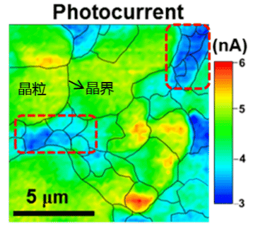
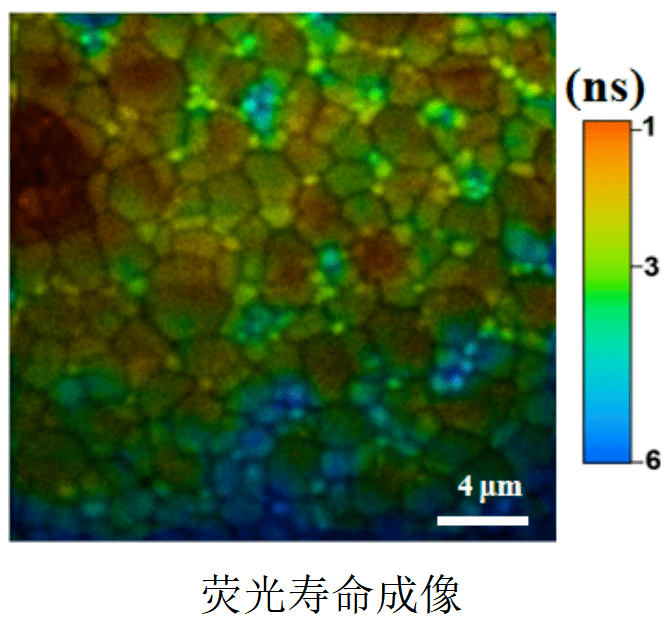
Fluorescence imaging system application examples explained 2 Multifunctional vibrating mirror scanning fluorescence imaging system, is a laser precision scanning, time-resolved acquisition and image

Fluorescence imaging system application examples explained Multifunctional vibrating mirror scanning fluorescence imaging system, is a laser precision scanning, time-resolved acquisition and image processing