Micro and Nano Processing | Introduction to Diffractive Optics
A DiffractiveOpticalElement (DOE) is a special optical component that deflects light to the m level at a precise angle θm and is expressed by the following equation:

A ray of light incident at an angle θi to the grating normal to the grating will diffract into one or more rays with an exit angle of θdm, θdm being a function of period Λ. where ni is the refractive index of the incident medium; nd is the refractive index of the outgoing medium; and m is the diffraction level, which for most applications is m = 1. Other different diffraction levels are given in Figure 1.1, but their diffraction efficiency is not indicated. For lenses, the efficiency of the other diffraction stages is minimized, except for the one you wish to use (usually the m=+1 stage).
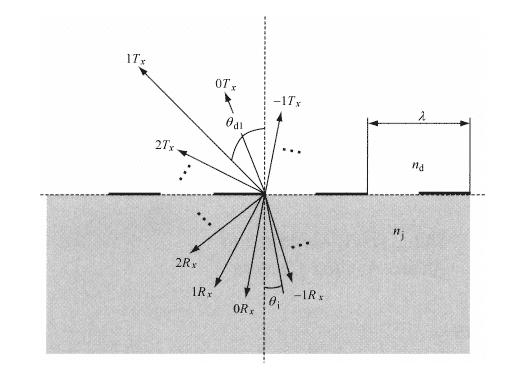
Figure 1.1 Angle of emergence as a function of grating period, refractive index and diffraction level (some transmission and reflection levels are given in the figure)
The period is a parameter for lateral control using lithography and can be specified in the technical requirements down to the nanometer level. For small aberration lenses, this particular control of the lateral position of the period would make DOE a more desirable part. For example, the general application of a lens is to converge light into a spot, and diffractive lenses can be designed and fabricated that can achieve diffraction-limited spot sizes. Figure 1.2 shows an 8th-order focusing lens capable of converging the phase front of a beam of parallel light incident at 2π-phase intervals to ensure that all of the light diffracted by the DOE is focused on a central point above the DOE at a distance F. The phase front required to focus the parallel beam is easily determined using the ray tracing procedure. The position and distance of each 2π discrete phase front corresponds to the period of each point position on the DOE. These values are entered into a CAD program and converted into a series of lithographic templates used in the DOE manufacturing process. The process is more complex, but easy to understand and the technology used is more mature.
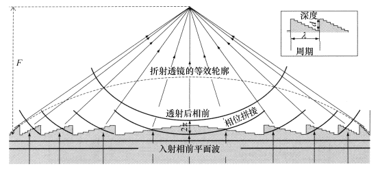
Figure 1.2 An 8th-order focusing lens (phase-front convergence of collimated beams every 2π phases apart to ensure that all beams diffracted by the DOE are incident on a center point above the DOE at a distance F)
We offer fastDiffractive Optical Elements (DOE) / Micro and Nanostructure Processing Design Services, Feel free to leave a message to inquire.
Related Products
Related Reading
Micro and Nano Processing | Electron Beam Lithography Processing Principle
Micro and Nano Processing | Electron Beam Lithography Principles and Available Optical Technologies
Micro and Nano Processing | Lithography - Focus on Ion Beam FIB
Micro and Nano Processing | Lithography - Fib Focused Ion
Micro and Nano Processing | Process Overview
Micro and Nano Processing | Thin Film Deposition, Photolithography, Etching Overview Nanofabrication Division

